MAX2062高线性,双模拟数字可变增益放大器(VGA)工作在50MHz至1000MHz的频率范围内,有两个独立的衰减器
️MAX2062 General Description:
MAX2062高线性,双模拟/数字可变/增益放大器(VGA)工作在50MHz至1000MHz的频率范围内,有两个独立的衰减器
每个信号路径。每个数字衰减器作为从外设控制,使用spi兼容接口或5位并行总线,总调节范围为31dB,步长为1dB。一个附加功能允许在四个步骤中的每一个步骤中进行快速增益选择,由用户通过spi兼容接口预编程。一个单独的2引脚控制,让用户快速访问任何一个自定义衰减状态,而无需重新编程SPI总线。每个模拟衰减器使用外部电压或通过使用片上8位DAC的spi兼容接口进行控制。
由于每个级都有自己的外部RF输入和RF输出,因此该组件可以配置为优化噪声系数(NF)(首先配置放大器),OIP3(最后配置放大器),或NF和OIP3的折衷。该器件的性能特点包括24dB放大器增益(仅放大器),最大增益时7.3dB NF(包括衰减器插入损耗),以及+41dBm的高OIP3电平。这些功能使该设备成为多路径接收器和发射器应用的理想VGA。
此外,该设备还可以通过单个+5V电源运行,具有完整的性能,也可以通过+3.3V电源运行,以增强节能模式,但性能较低。该器件采用紧凑型48针TQFN封装(7mm x 7mm),带有外露的衬垫。在从TC =-40NC到+85NC的扩展温度范围内,电气性能得到保证。
The MAX2062 high-linearity, dual analog/digital variable/gain amplifier (VGA) operates in the 50MHz to 1000MHz frequency range with two independent attenuators in
each signal path. Each digital attenuator is controlled as a slave peripheral using either the SPI-compatible interface, or a 5-bit parallel bus with 31dB total adjust-ment range in 1dB steps. An added feature allows rapid-fire gain selection among each of the four steps, preprogrammed by the user through the SPI-compatible interface. A separate 2-pin control lets the user quickly access any one of four customized attenuation states without reprogramming the SPI bus. Each analog attenu-ator is controlled using an external voltage or through the SPI-compatible interface using an on-chip 8-bit DAC.
Since each of the stages has its own external RF input and RF output, this component can be configured to either optimize noise figure (NF) (amplifier configured first), OIP3 (amplifier last), or a compromise of NF and OIP3. The device’s performance features include 24dB amplifier gain (amplifier only), 7.3dB NF at maximum gain (includes attenuator insertion losses), and a high OIP3 level of +41dBm. Each of these features makes the device an ideal VGA for multipath receiver and trans-mitter applications.
展开全文In addition, the device operates from a single +5V supply with full performance or a +3.3V supply for an enhanced power-savings mode with lower performance. The device is available in a compact 48-pin TQFN package (7mm x 7mm) with an exposed pad. Electrical performance is guaranteed over the extended tempera-ture range, from TC =-40NC to +85NC.
️MAX2062 Features:
Independently Controlled Dual Paths
50MHz to 1000MHz RF Frequency Range
Pin-Compatible Family Includes
MAX2063 (Digital-Only VGA)
MAX2064 (Analog-Only VGA)
19.4dB (typ) Maximum Gain
0.34dB Gain Flatness Over 100MHz Bandwidth
64dB Gain Range (33dB Analog Plus 31dB Digital)
56dB Path Isolation (at 200MHz)
Built-In 8-Bit DACs for Analog Attenuation Control
Supports Four Rapid-Fire Preprogrammed
Attenuator States
Quickly Access Any One of Four Customized
Attenuator States
Ideal for Fast-Attack, High-Level Blocker
Protection
Protects ADC Overdrive Condition
Excellent Linearity (Configured with Amp Last at 200MHz)
+41dBm OIP3
+56dBm OIP2
+19dBm Output 1dB Compression Point
7.3dB Typical Noise Figure (at 200MHz)
Fast, 25ns Digital Switching
Very Low Digital VGA Amplitude Overshoot/Undershoot
Single +5V Supply (or+3.3V Operation)
Amplifier Power-Down Mode for TDD Applications
️MAX2062 Applications:
IF and RF Gain Stages
Temperature-Compensation Circuits
GSM/EDGE Base Stations
WCDMA, TD-SCDMA, and cdma2000M Base
Stations
WiMAXM, LTE, and TD-LTE Base Stations and
Customer-Premise Equipment
Fixed Broadband Wireless Access
Wireless Local Loop
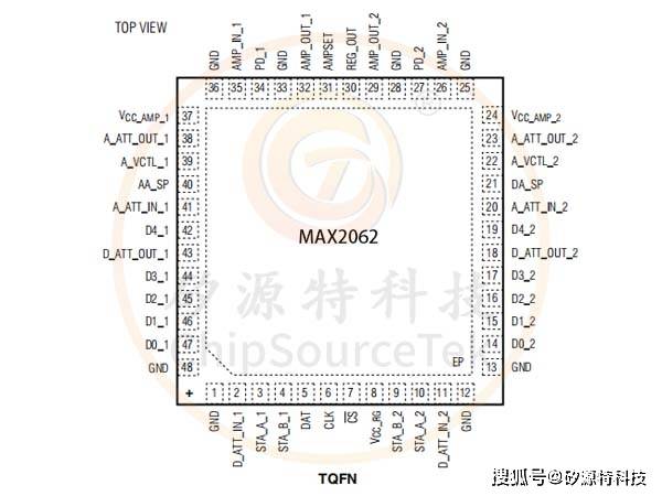
️MAX2062 Pin Configuration:
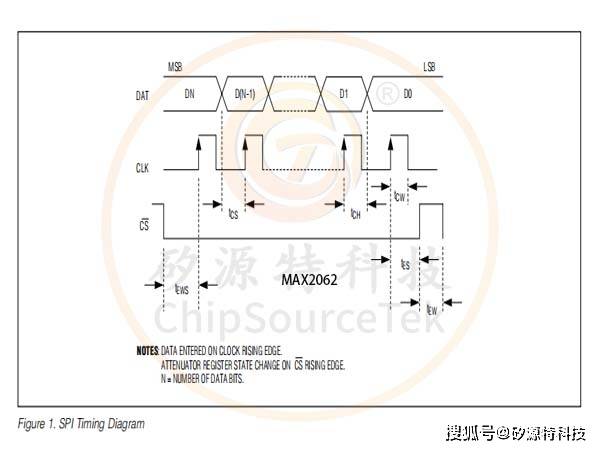
️MAX2062 SPI Timing Diagram:
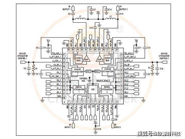
️MAX2062 Typical Application Circuit: